Guide to the TD4 4-bit DIY CPU
I bought a cute little 4 bit cpu kit from Aliexpress called the TD4. It has 2 registers, some LEDs, and 16 bytes of program ROM. Quite limited but still very cool and teaches a lot of principles of computer architecture.
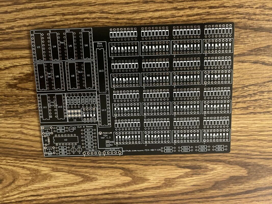
The documentation, schematics, and pictures for this cpu are here https://github.com/wuxx/TD4-4BIT-CPU. It’s a little sparse though. I can imagine a student getting overwhelmed. So I thought it would be helpful to write some longer form notes.
Building
We took two sessions just soldering it up.
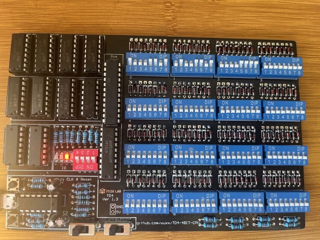
This image 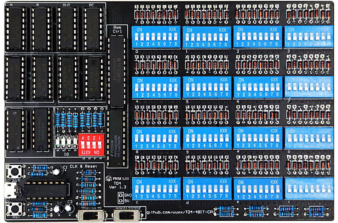
plus the schematic were enough instructions such that it wasn’t too hard.
The directionality of the surface mount diodes gave us pause, but we used a diode tester functionality in our multimeter to figure it out. The tiny green line on the front of the diode is towards the bottom of the board. I believe the line was on the back of the diode was towards the top, but it is soldered down now so I can’t check.
The thing that gave us the most trouble was soldering on the USB connector. I’d advise doing this before putting on the IC sockets, because it got in the way of the iron. The middle pins of the USB are unconnected, so you can just blast them if need be. The USB is only for power.
Which chip goes where can be seen by inspecting the schematic for part number and IC number. The notch aligns with the notch printed on the PCB board. It basically worked the first time, minus an intermittent power connection on the usb.
Soldering all those diodes sucked.
How it Works
At a a high level here’s how it works
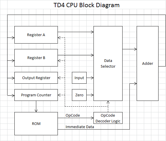
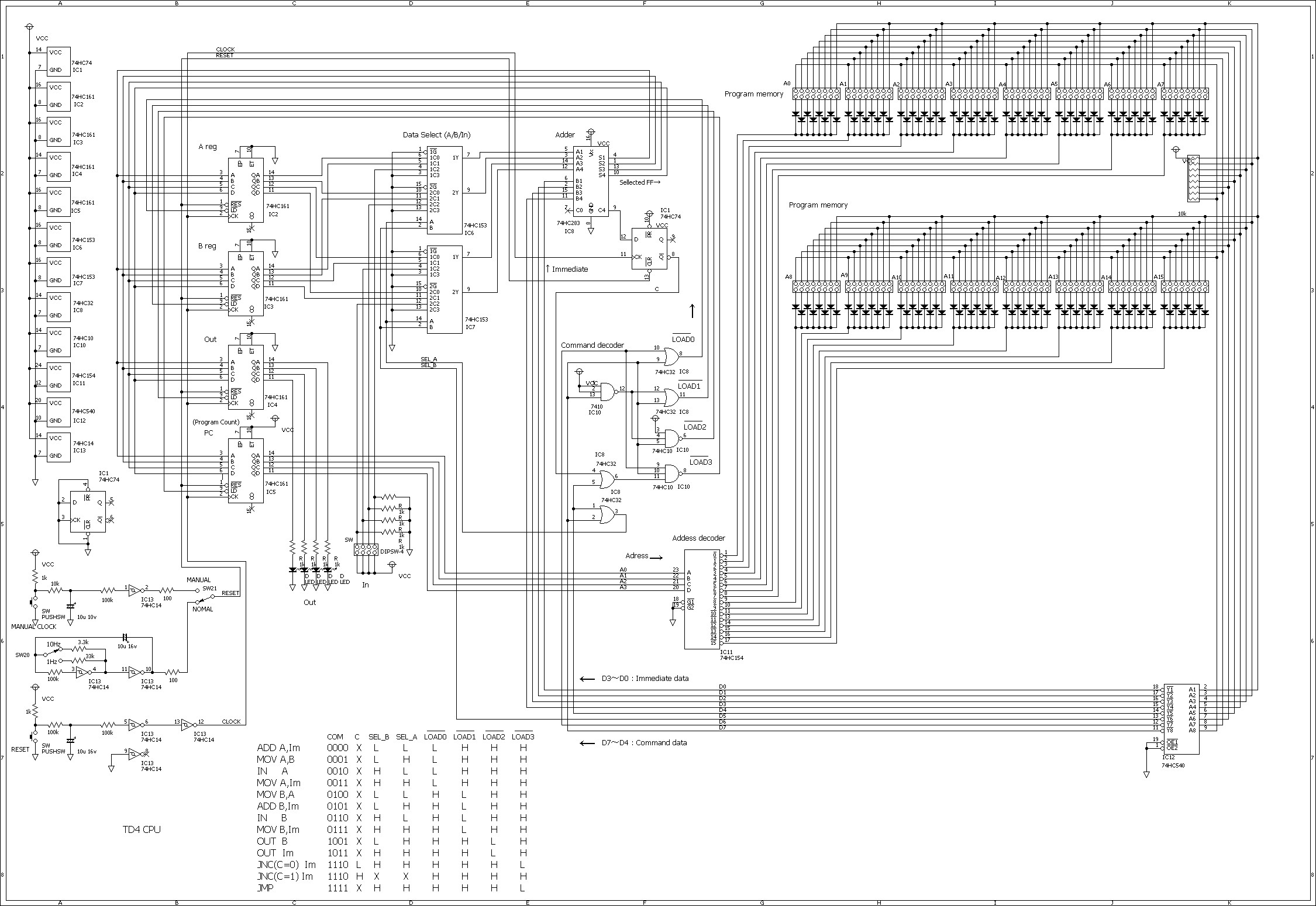
The program ROM is a bank of 16 dip switches. This is the entire size of programs available to you, which makes it tricky to do much. Pins 5-8 of each dip switch are an opcode, selecting between ADD, MOV, IN, OUT, JNC, JMP instructions. These bits go through some combinatorial circuit to control
- What signal enters the addition unit (input operand of instruction)
- Which register latches in the output of the addition unit. (The output operand of the instruction)
Bits 1-4 of the dip switch are the immediate value for the instruction, which is always piped into the adder.
The data selector can also select a hard wired zero signal (ground). This is used for example by the MOV A,Im instruction. This MOV instruction is implemented by adding Im to 0 and clocking the result into A.
The order of the immediate and command bits is a bit confusing. Sometimes it feels like they are reversed. The least significant bit is the low labelled one on the dip switch. For example, the value 3 is entered in as 1100 on the first 4 bits of the dip switch.
A Little Deeper
Address Decoder
The address decoder chip IC11 is a demultiplexer that takes in 4bit signal and drives the one of it’s 16 output signals low that corresponds to this number. When driven low, current can flow through that dip bank’s diodes if the dip switch is connected. Otherwise, pullup resistors R21-R26 keep the signal high.
IC12 is essentially a buffering inverter circuit for the result of the ROM.
Command Decoder
The command bits are translated by discrete combinatorial logic chips in IC8 and IC10 into not_LOAD0,1,2,3 and SEL_A/SEL_B signals. Really, not_LOAD0,1,2,3 could be called not_LOADA,B,Out,PC since that is what they are hooked up to.
| instruction | bit7-bit4 | bit3-bit0 | C | SEL_B | SEL_A | #LOAD0/A | #LOAD1/B | #LOAD2/IN | #LOAD3/PC |
|---|---|---|---|---|---|---|---|---|---|
| ADD A, Im | 0000 | Im | X | L | L | L | H | H | H |
| MOV A, B | 0001 | 0000 | X | L | H | L | H | H | H |
| IN A | 0010 | 0000 | X | H | L | L | H | H | H |
| MOV A, Im | 0011 | Im | X | H | H | L | H | H | H |
| MOV B, A | 0100 | 0000 | X | L | L | H | L | H | H |
| ADD B, Im | 0101 | Im | X | L | H | H | L | H | H |
| IN B | 0110 | 0000 | X | H | L | H | L | H | H |
| MOV B, Im | 0111 | Im | X | H | H | H | L | H | H |
| OUT B | 1001 | 0000 | X | L | H | H | H | L | H |
| OUT Im | 1011 | Im | X | H | H | H | H | L | H |
| JNC Im | 1110 | Im | L | H | H | H | H | H | L |
| JNC Im | 1110 | Im | H | X | X | H | H | H | H |
| JMP Im | 1111 | Im | X | H | H | H | H | H | L |
Data Selector
SEL_A and SEL_B are wired into the data selector chips IC6 and IC7. They select from 4 possible options,
| A | B | In Operand |
|---|---|---|
| 0 | 0 | A |
| 0 | 1 | B |
| 1 | 0 | In |
| 1 | 1 | Zero |
The Zero signal is hardwired to ground.
Adder
The 4 bits selected output to the Adder chip IC8, which also receives the immediate bits1-4 from the ROM bank selected. A side note, The immediate bits are read by more instructions than might be apparent from their pneumonic. For example, OUT B actually still adds in the immediate. This functionality could be useful but also confusing. By default, zero out the immediate bits if you don’t want them.
Registers
The registers A,B,Out,PC are all counter chips. Only PC has the counting functionality enabled. On the edge of the clock signal, if the not_LOADx signal is low, data will latch in from pins A,B,C,D into the output pins QA,QB,QC,QD. JMPs are implemented by moving values into the PC register, which is fed back into the ROM address decoder.
Carry Flip Flop
An interesting piece is the Carry circuit which has a D flip flop for storing the overflow carry bit from the previous operation. This is needed to implement the JNC “jump if no carry” functionality. This operates by feeding into the command decoder circuit and disabling the LOADPC coming from the instruction if there is a carry.
Note that there appears to be a error on this version of the schematic for the command decoder. Can you find it?
Clock
Down in the bottom right is the clock circuit. The switches change from manual clock to auto clock and also change the clock speed. The clock is a RC controlled multivibrator. I haven’t actually seriously analyzed it.
Simple Programs
We ran a couple experimental programs. First its good to try something very simple.
For reference again, this is the instruction set
| instruction | bit7-bit4 | bit3-bit0 |
|---|---|---|
| ADD A, Im | 0000 | Im |
| MOV A, B | 0001 | 0000 |
| IN A | 0010 | 0000 |
| MOV A, Im | 0011 | Im |
| MOV B, A | 0100 | 0000 |
| ADD B, Im | 0101 | Im |
| IN B | 0110 | 0000 |
| MOV B, Im | 0111 | Im |
| OUT B | 1001 | 0000 |
| OUT Im | 1011 | Im |
| JNC Im | 1110 | Im |
| JMP Im | 1111 | Im |
Output to LED
Try getting this program to work OUT 0101
Looking up the opcode for OUT Im on the table it is 1011.
This translated to the first dip switch being in 1010 1101 The first piece is the constant immediate, and the second piece is the reverse of that opcode.
Simple Flashing
Now we can try a simple blinking program with a jump.
We output two different constants and then JMP back to instruction 0
Which translates to
         # Im   | Com
         #------|-----
OUT 0001 # 1000 | 1101
OUT 0010 # 0100 | 1101
JMP 0    # 0000 | 1111
Counting Up
Now we can trying counting
ADD B 1
OUT B
JMP 0
Counting Down
Counting down can be done once you realize that adding 15 is the same as subtracting 1 modulo 16. require realizing modular arithmetic
ADD B 15
OUT B
JMP 0
Counting Up then Down
This is much trickier strangely. We screwed up a lot getting this simple program to work. In our defense we were tired. But remember to update your jump addresses, put things in the right order, manually assemble, it’s a lot.
Mistakes we made
- we fed will ice cream too early.
- We flipped the labels going into JNC vs JMP
- We had the OUT in places they couldn’t be executed (at the bottom of the program)
- We moved OUT after the add, destroying the carry for ADD A 1
- We realized we should think of ADD B 1, OUT B a a single unit. A pseudoinstruction.
- And in fact after examining the circuit, thee two can be compressed to OUT B 1 because OUT actually takes immediates. We lucked out that we zeroed the immediates on MOV and OUT.
Remember the program counter was 0 indexed
00: ADD B 1     1000 1010
01: OUT B       xxxx 1001
02: MOV A B     xxxx 1000  # test if at 15
03: ADD A 1     1000 0000  # adding 1 to 15 makes a carry
04: JNC 0       0000 0111  # jump to 0 if no overflow (B != 15)
05: ADD B 15    1111 1010  # Go down 1 by adding 15
06: OUT B       xxxx 1001
07: MOV A B     xxxx 1000  # test if at 0
08: ADD A 15    1111 0000  # only 0 does not overflow when add 15
09: JNC 0       0000 0111  # jump to ascending at 0 if not overflow (B = 0)
10: JMP 5       0110 1111  # default jump to 5
An alternative possibly buggy version. Using the idea JC ~ JNC;JMP and can we directly test the overflow on B without using A as scratch? Do we miss some numbers though? The ends of the loop are tricky.
00: ADD B 1
01: JNC 3
02: JMP 5
03: OUT B
04: JMP 0
05: MOV B 15
06: ADD B 15
07: JNC 0
08: OUT B
09: JMP 6
Python Assembler and Simulator
Here’s a little python simulator and assembler that Ben and I slammed out. Well, Ben mostly wrote. Maybe using regex like this is a bit goofy. Maybe its nice? match statements rule. We should return to this and make it better, but it’s a start.
There is also an assembler in the TD4 repo but I haven’t tried using it.
import re
from collections import namedtuple

from types import SimpleNamespace

instruction_regex = re.compile(r"(?P<cmd>ADD|OUT|MOV|JMP|JNC|IN) +(?P<arg1>A|B|\d{1,2})(?: +(?P<arg2>A|B|\d{1,2}))? *(?:#.*)?")

input = """\
ADD B 1
OUT B
MOV A B
ADD A 1
JNC 0
ADD B 15
OUT B
MOV A B
ADD A 15 # this is a comment
JNC 0
JMP 5\
"""

NULL_IM = "0000"

def im_to_str(im):
    return f"{int(im):04b}"[::-1]

# Assembler
# We made an error on ADD B not updtang something copied from ADD A
program = []
for line in input.split("\n"):
    instruction = instruction_regex.fullmatch(line)
    match instruction["cmd"], instruction["arg1"], instruction["arg2"]:
        case "ADD", "A", im:
            program.append(im_to_str(im)+"0000"[::-1])
        case "MOV", "A", "B":
            program.append(NULL_IM+"0001"[::-1])
        case "IN", "A", None:
            program.append(NULL_IM+"0010"[::-1])
        case "MOV", "A", im:
            program.append(im_to_str(im)+"0011"[::-1])
        case "MOV", "B", "A":
            program.append(NULL_IM+"0100"[::-1])
        case "ADD", "B", im:
            program.append(im_to_str(im)+"0101"[::-1])
        case "IN", "B", None:
            program.append(NULL_IM+"0110"[::-1])
        case "MOV", "B", im:
            program.append(im_to_str(im)+"1001"[::-1])
        case "OUT", "B", None:
            program.append(NULL_IM+"1001"[::-1])
        case "OUT", im, None:
            program.append(im_to_str(im)+"1011"[::-1])
        case "JNC", im, None:
            program.append(im_to_str(im)+"1110"[::-1])
        case "JMP", im, None:
            program.append(im_to_str(im)+"1111"[::-1])
        case _:
            raise Exception("Unrecognized command")

print(program)

# Simulator
State = namedtuple("State", "a, b, out, pc, c, inp, program")

def build_starting_state(program):
    return State(0,0,0,0,0,0,program)

starting_state = build_starting_state("""\
ADD B 1
OUT B
JMP 0\
""".split("\n"))


def step(state):
    a, b, out, pc, c, inp, program = state
    instruction = instruction_regex.fullmatch(program[pc])
    match instruction["cmd"], instruction["arg1"], instruction["arg2"]:
        case "ADD", "A", im:
            im_int = int(im)
            assert 0 <= im_int < 16
            a_tmp = a+im_int
            return State(a_tmp%16, b, out, (pc+1)%16, a_tmp>=16, inp, program)
        case "MOV", "A", "B":
            return State(b, b, out, (pc+1)%16, False, inp, program)
        case "IN", "A", None:
            return State(inp, b, out, (pc+1)%16, False, inp, program)
        case "MOV", "A", im:
            im_int = int(im)
            assert 0 <= im_int < 16
            return State(im_int, b, out, (pc+1)%16, False, inp, program)
        case "MOV", "B", "A":
            return State(a, a, out, (pc+1)%16, False, inp, program)
        case "ADD", "B", im:
            im_int = int(im)
            assert 0 <= im_int < 16
            b_tmp = b+im_int
            return State(a, b_tmp%16, out, (pc+1)%16, b_tmp>=16, inp, program)
        case "IN", "B", None:
            return State(a, inp, out, (pc+1)%16, False, inp, program)
        case "MOV", "B", im:
            im_int = int(im)
            assert 0 <= im_int < 16
            return State(a, im_int, out, (pc+1)%16, False, inp, program)
        case "OUT", "B", None:
            print(b)
            return State(a, b, b, (pc+1)%16, False, inp, program)
        case "OUT", im, None:
            im_int = int(im)
            assert 0 <= im_int < 16
            print(im_int)
            return State(a, b, im_int, (pc+1)%16, False, inp, program)
        case "JNC", im, None:
            im_int = int(im)
            assert 0 <= im_int < 16
            return State(a, b, out, im_int if not c else (pc+1)%16, False, inp, program)
        case "JMP", im, None:
            im_int = int(im)
            assert 0 <= im_int < 16
            return State(a, b, out, im_int, False, inp, program)
        case _:
            raise Exception("Unrecognized command")


state = starting_state
print(state)
for _ in range(200):
    state = step(state)
Bits and Bobbles
If you find this intriguing you may want to check out two related projects:
We had a blast a few years ago taking the Nand2Tetris course https://www.nand2tetris.org/. In it, you learn how to design a computer from gates up to a small programming language. It is a good reference for background on what is going on in the TD4.
Another option is the Ben Eater computer https://eater.net/8bit/. The kits are quite a bit more expensive, the cpu is more complex/powerful, and there is a lot more material.
It seems like there is a japanese book about this thing but I can’t find a translation
Examining the schematic, looks like there is no ram to speak of, so this is a very limited machine. A + B + OUT + PC means there is 16 bits of state? Can easily exhaustively check this for anything you’d like. What about synthesizing programs? Maybe this is good though This is so constrained it feels more like a finite state machine. Try model checking it?
Could I implement in python hdl or verilog or that gui thing?
some further things to try
- subtraction
- equality checking. Bounded model checking
- suproptimization
Didn’t Conor Mcbride have a 4 bit cpu videos? Are there actually 4-bit cpu ou there like this?
https://en.wikipedia.org/wiki/4-bit_computing
What interesting programs can be written? Toughy.
Model each chip
module ALU()

end

module ROM()
end


`def JMP 0

module Computron()
    reg [3:0] A;
    reg [3:0] B;
    reg [3:0] OUT;
    reg [3:0] PC;


end

module HC153(in[4], out[16]); // demultiplexer


endmodule;
74HC154 - Address decoder - 4 - 16 line decoder / demultiplexer. The four incoming signals are translated to 16 mutually exclusive outputs. For example in the inputs pins are LLHH will draw pin 3 of the output low. Because of all the diodes, only current will flow in through the ROM switches when that bank is enabled by bing drawn low
The two enable pins are drawn down to ground so that output is always enabled.
The lines come into this decode and select which flipy floppr is drawn
74HC540 is an inverting buffer.


https://github.com/wuxx/TD4-4BIT-CPU
https://en.wikipedia.org/wiki/Charlieplexing Are all these diodes chaliplexed? Nope. Nevermind.
https://hackaday.io/project/8442-ttl-based-4-bit-cpu https://hackaday.io/project/26215-td4-cpu http://kamakurium.com/wp-content/uploads/2016/01/cpu_td4 http://visual6502.org/ http://www.4004.com/


# here we made  failed attempt to emulate at the circuit level. Maybe we'll come back to this.

# This is wrong.
def counter(a, b, c, d, not_load, not_reset, count_enable):
    load = not not_load
    reset = not not_reset
    if reset:
        return 0, 0, 0, 0
    if load:
        return a, b, c, d
    inp = a + (b << 1) + (c << 2) + (d << 3)
    inp += 1
    inp %= 16
    a = inp & 1
    b = (inp >> 1) & 1
    c = (inp >> 2) & 1
    d = (inp >> 3) & 1
    return a, b, c, d

assert(counter(1,1,1,1,0,1) == 1,1,1,1)
assert(counter(1,1,1,1,1,1) == 0,0,0,0)
assert(counter(1,1,1,1,1,0) == 0,0,0,0)

def multiplexer(c0, c1, c2, c3, a, b):
    match a, b:
        case False, False:
            return c0
        case False, True:
            return c1
        case True, False:
            return c2
        case True, True:
            return c3


def flip_flop(d, not_clr):
    clr = not not_clr
    if clr:
        return False, True
    return d, not d

def adder(a0, a1, a2, a3, b0, b1, b2, b3):
    a_int = a0 + (a1 << 1) + (a2 << 2) + (a3 << 3)
    b_int = b0 + (b1 << 1) + (b2 << 2) + (b3 << 3)

    s_int = a_int + b_int

    s0 = s_int & 1
    s1 = (s_int >> 1) & 1
    s2 = (s_int >> 2) & 1
    s3 = (s_int >> 3) & 1
    carry_out = (s_int >> 4) & 1

    return s0, s1, s2, s3, carry_out

# We found a bug in one of the diagrams. It showed
def command_decoder(d4, d5, d6, d7, not_c):
    sel_a = d4 or d7
    sel_b = d5
    not_load0 = d6 or d7
    not_load1 = (not d6) or d7
    not_load2 = not ((not d6) and d7)
    not_load3 = not ((not_c or d4) and d6 and d7)
    return not_load0, not_load1, not_load2, not_load3, sel_a, sel_b

def rom():
    ...

def circuit_step(state):
    a, b, out, pc, c, inp, program = state

    adder0, adder1, adder2, adder3 = adder()
    a_val = counter(adder0, adder1, adder2, adder3, not_load0)
    b_val = counter(adder0, adder1, adder2, adder3, not_load0)
    out_val = counter(adder0, adder1, adder2, adder3, not_load0)
    pc_val = counter(adder0, adder1, adder2, adder3, not_load0)
    new_state = State(a_out, b_out, out_out, ...)
Use lark?
prog = """

ADD B 1
"""

{
    "ADD": "1000",
    "OUT": "1001",
    "MOV": "1010",
    "JNC": "0111",
    "JMP": "1111"
}

def assemble(x):
    op = x[0]
    match x:
        case "MOV":
        case "ADD":
        case "OUT":
        case "JNC":
        case "JMP":
        case _:
            raise ValueError(f"Unknown op {op}")

grammar = """
    "ADD"
    "MOV"
    "JNC"
    "OUT"
    "JMP"
    "JNC"
    "@" name
 -> label

"""
```